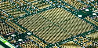
Keys to Design a Successful HDI PCB
HDI is an acronym for High-Density Interconnect, which is a modern type of printed circuit boards PCBs which was started to develop at the end of the 20th century. In common, PCB boards, mechanical drilling is used, which arises some disadvantages like high cost with high, size which and improvement is challenging due to the influence of drilling tools. However, for HDI PCBs, laser drilling is used. As soon as HDI is introduced in the market, it gets too much popularity. HDI boards are also recognized as laser boards. It comes up with a small size but high functionality. HDI Technology brings the PCB industry on the rise and almost all electronic devices use PCBs these days.
In terms of HDI board design as compared to the common PCBs, the major difference is that HDI PCBs make interconnection because of the blind holes and buried holes in place of through holes. Additionally, the small space and finer lines are also utilized in the PCB designs. However, HDI PCB Manufacturers must know how to place all the necessary components in the small space at HDI PCB boards, how to switch the arrangement of blind holes and through holes, and the entire manufacturing process.
Manufacturing Process
The HDI manufacturing process is mentioned below:
Aperture
Aperture ratio should be considered in through holes, blind holes, and in buried holes. For usual mechanical drilling in common PCBs, through hole aperture should be above 0.15mm and the thickness-to-aperture ratio of the board should be 8:1. However, for laser drilling in HDI, the aperture of the laser hole must be in the range of three to 6mil
While the plating filling hole depth to the aperture must be 1:1.
Remember that the thicker the board is the small the aperture is. During the process of plating, it is hard for the chemical solution to enter deep into the drilling holes. Therefore, the circuit-platting device forces the solution to the center of the holes by pressing. Concentration gradients make the plating thing, which results in a slight circuit aperture on the layer of holes. When the volt increases or the board go through environmental impact, errors, and issues become more obvious which results in circuit failure or breakage. Therefore, HDI PCB manufacturers must know the techniques to fix the issues in the design.
Stack
Stack up in the HDI PCB layer can be categorized based about layers with blind holes. Some of the common categories are mentioned below:
- 1-HDI with buried holes
- Non-stacked 2-HDI with buried holes
- Stacked but non-resign filled 2-HDI
- Stacked and resign filled 2-HDI
Pressure and temperature commonly affect the boards in the process of stacking up after that there is still strain on the board. The strain on either side of the board is nonuniform if the stacked boards are asymmetric then one-sided warpage is established which extremely decreases board yield.
Process Flow
4-layer HDI with 1 stacking
The process flow with 4 layers is the same as with a common PCB excluding the sequence of drilling holes. First mechanical drilling comes with buried holes of 2-3 layers, then the mechanical through holes of 1-4 layers, then 1-2 blind holes, and 4-3 blind holes.
6-layers HDI with two stacking
The system goes with the flow of 6-layer HDI with two stacking is comparable with that of a normal PCB barring the sequence of drilling holes. First comes mechanical drilling of buried holes on 3-4 layers, then comes drilling of the buried gap on 2-5 layers, then blind holes on 2-3 layers and 5-4 layers, then thru holes on 1-6 and ultimately come the drilling of 1-2 blind gap and 6-5 blind hole. If you want to know more you can visit Mad PCB


